The Silicon Photomultiplier (SiPM) Concept and Design Development
11 March 2015
by Sergey Vinogradov
Senior Marie Curie Research Fellow at the Dept. of Physics, University of Liverpool and the Cockcroft Institute of Accelerator Science and Technology, UK
Detection of optical light pulses with photon number resolution starting from single photons, was an ultimate goal of R&D in photodetectors for more than half a century. Vacuum photomultiplier tubes (PMTs), semiconductor avalanche photodiodes (APDs) and Geiger-mode APDs or so-called single photon avalanche diodes (SPADs) have been invented, developed and successfully utilized for low light level detection approaching to this goal by different technologies. However, all these devices are unable to provide a complete solution to a problem of photon number resolving detection at room temperature. In order to detect one photon, a detector has to produce measurable electrical signal above electronic noise of the acquisition circuit, which is about 10,000 electrons at the bandwidth of 1 GHz. It means that besides conversion of photons to electrons, a multiplication of the electrons with a very high gain (>10,000) is required to get timing certainty of the detection of about 1 ns.
In turn, multiplication mechanisms of these devices are inherently noisy producing from a single electron at the input a random number of electrons at the output. It means that two photons could hardly be resolved if the multiplication noise is comparable with the mean gain; that situation is typical for PMTs and much worse for conventional linear mode APDs. In contrast, an avalanche process in a SPAD with active quenching of a Geiger-mode breakdown could be considered as a practically noiseless multiplication with a pre-defined gain, but as a binary detector SPAD is unable to detect multi-photon pulse. The attempt to mitigate this by using an array of SPAD pixels fails since active quenching circuitry occupies a lot of space around every pixel resulting in a low fill factor of the array (~ 10%) and dramatic losses of incident photons.
SiPM technology represents an unprecedented attempt to create an ideal solid-state photon detector solving a double trade-off of avalanche processes: the higher multiplication gain inevitably results in higher multiplication noise, as well as, in longer multiplication time (the lower bandwidth). The idea on how to harness a high gain avalanche in such a way so as to make it as fast and noiseless as possible, originated from basic studies of over-breakdown avalanche processes in Metal-Insulator-Semiconductor (MIS) structures. These studies were carried out since the mid-1970s in the Lebedev Physical Institute, Moscow, Russia, in the Solid State Photodetectors group led by Dr. V. Shubin. It was found that charge carriers generated in an avalanche filament and accumulated at semiconductor-insulator interface, provide a self-quenching of a breakdown with self-calibrating of an avalanche charge due to screening of an electric field into the avalanche filament region; moreover, the higher over-breakdown voltage the lower charge fluctuations. So, this approach (known as Avalanche with Negative Feedback, ANF) assumes that an avalanche breakdown as a positive feedback process should be self-suppressed by accumulation of an avalanche charge as a negative feedback process, and both processes should be as strong as possible to get fastest and noiseless result.
However, MIS structures could be super-sensitive to photons only during non-stationary depletion of the semiconductor region adjacent to an insulator layer and it requires ramping bias voltage and synchronous gated detection of optical signals. In order to provide more convenient free-running mode of operation at DC bias voltage, a blocking insulator (SiO2) has been substituted to “insulator with leakage” – wide band gap semiconductor (SiC) and other resistive materials. Another key modification with respect to an initial non-structured planar design of MIS detectors was a separation of an active area into elements or pixels which localize and separate avalanche filaments. These improvements have been introduced by Dr. Z. Sadygov and his colleagues at the INR/MELZ collaboration. Thus, applying the ANF concept to DC operating structures of multi-pixel architecture of various designs, a new generation of high-gain low-noise avalanche detectors have been developed in Russia in the late 1980s – early 2000s. They are known by different names as Metal-Resistor-Semiconductor (MRS) APD, ANF APD, Solid State Photomultiplier (SSPM), Micro-pixel APD, and SiPM.
The most popular detector from this generation – SiPM – has been developed by the MEPhI/Pulsar collaboration led by Prof. B. Dolgoshein. The SiPM of this kind was very attractive due to the simplicity of its design and the ability to be reliably produced using semiconductor technology of moderate level. The negative feedback element in SiPM was realized as a thin-film polysilicon strip resistor connecting each individual APD pixel to a common electrode and located between pixels.

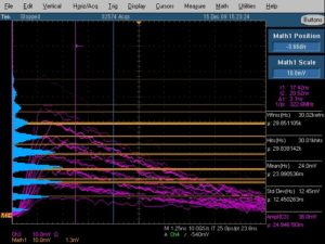
Photon number resolving response of SiPM (Hamamatsu MPPC) to short multi-photon light pulse (S. Vinogradov)
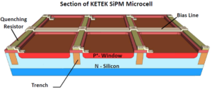
Since the mid-2000s, the SiPM design with polysilicon resistors became a conventional ground for an emerging wave of SiPM developments by Hamamatsu Photonics, SensL, FBK, STMicroelectronics, Excelitas Technologies, KETEK, and some others.
So, after all, the SiPM appears to be rather similar to a SPAD array with passive quenching, but with a much faster pixel recovery and much higher fill factor. In turn, the success of SiPM technology has inspired the re-invention of a SPAD array detector, using the achievements of modern CMOS technology and advancing its readout architecture in the so-called digital SiPM (dSiPM) developed by Philips in 2009, where the main drawback of SPAD arrays – low fill factor – was improved to about 50%.
The ANF concept and SiPM technology were also accepted by developers of non-silicon, first of all, the near-infrared (NIR) APDs starting since the mid-2000s in the USA. The designs have been adapted to III-V compound technology utilizing negative feedback based either on thin film resistor (Princeton Lightwave) or on charge accumulation at heterointerfaces of III-V layers (Jet Propulsion Laboratory, UCSD, UCLA).
Recently, an expansion of the SSPM into ultraviolet (UV) wavelengths and harsh environment operation has been possible through the development of a SiC-based UV SSPM (GE Global Research Center, 2014).
The overwhelming success and worldwide recognition of SiPM technology are due to its unprecedented performance at room temperature in a photon number resolution of multi-photon pulses, as well as, to its arrival time resolution. Highly beneficial features are the low operating voltages, insensitivity to magnetic field and to nuclear counter effect, scalability in creating large arrays, and its robustness and reliability for years, unaffected by occasional over-lighting. Now SiPM is approaching to be a real working horse for a variety of scientific and industrial applications, and mass-production pricing facilitates this progress.
However, conventional SiPM design has some drawbacks, for example the trade-off between density of pixels (dynamic range) and fill factor (detection efficiency), multiple trade-off dealt with pixel area – gain – pulse width – recovery time – crosstalk – after pulsing. Some of them are subjected to ongoing countermeasures and improvements, and some are inherent ones. There is room for alternative designs, thus a number of proprietary designs have been developing so far (Zecotek, Max Plank Institute, Novel Device Laboratory, ASTAR Institute of Microelectronics, and some others).
Further reading:
V. Saveliev, “Silicon Photomultipliers – New Era of Photon Detection”, ch. 14 in Advances in Optical and Photonic Devices, InTech, pp. 249–272 (2010)
Submitted by Eleni Chatzichristou
APPEC Communications Officer


